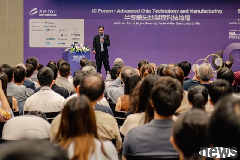
Applied Materials (hereinafter referred to as "Appliance") presents key technologies for advanced packaging, process innovation and continuous development at the SEMICON Taiwan 2025 International Semiconductor Exhibition Forum. Yu Ding-yu, Vice President of the Escort Group and President of the Taiwan District, pointed out that Escort’s unique integrated materials engineering solution will help customers improve yields, accelerate product launch speed, promote sustainable development, and at the same time improve chip efficiency. "By realizing the next generation of chip innovation, Escort is injecting dynamics into the AI era and reshaping the future of computing technology."
In order to face the most complex technical challenges in the semiconductor industry and to create the next generation of AI chips, we propose four major solutions.
First, with the AI chip scales that are 2 mega transistors, which are far beyond the limit of current process technology, and the challenges of chip microfilm processing surface splicing, positioning and slimming errors, E-Material has launched the "Digital Lithography Technology" (DLT) for maskless and GPU drive computing, with a key size uniformity of less than 2 microns and a 0.5 micron combination accuracy, achieving the unique integration of the AI packaging of mega-level transistors.
Second, innovation of advanced logical components and materials for 2 nanometers and more, provides breakthrough materials and process innovations to meet the semiconductor needs of AI drives. By leading solutions in the fields of hard mask patterning, low impedance metallization, precision planarization and quantity measurement, it has helped wafer manufacturers improve efficiency and yield in advanced processes of 2 nm and more. In addition, the equipment also introduces the common optimization architecture of all-round material components and circuit systems in the forum, aiming to comprehensively improve the efficiency of various chips.
Third, as the industry moves from system single wafers to system-level packaging, the surface materials promote the heterogeneous integration process through key technologies, such as hybrid bonding, silicon perforation, fanout, convex, silicon photons and rectangular substrates, to accelerate innovation and drive the future development of AI and advanced computing.
Finally, the 2040 Pure Zero Strategy should challenge the carbon reduction challenge of semiconductor industry. Yingcai pointed out that the company adopts quantitative and system-level strategies, focusing on providing solutions and services to reduce the energy consumption and carbon emissions of the wafer factory without affecting operation efficiency. These measures aim to promote the continuous development of scale and value chains, and demonstrate the commitment to the climate action of semiconductor industry.
Extended reading: Apple, Qualcomm? NVIDIA is expected to become the first customer of Taiwan A16 Called NVIDIA violated the anti-imperial method! China: Implement further investigations in accordance with the law