Chen Shilong said in his speech that this move will help companies overcome the high capital threshold, which is also the main challenge facing when converting technology. Through this facility, local SMEs and starting companies can use the services provided by the center to accelerate product development and production and launch products on the market faster.
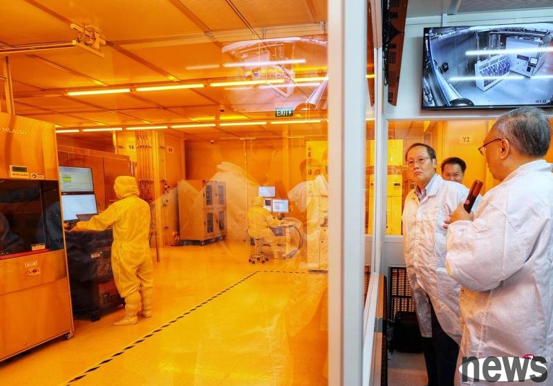
Dr. Chen Shilong, Minister of Human Resources, in charge of Energy and Technology, made the above announcement when attending the opening ceremony of the National Semiconductor Translation and Innovation Centre for Gallium Nitride (NSTIC (GaN)) on Thursday (June 26). This is also the first local facility to produce six-inch and eight-inch gallium nitride wafers simultaneously.
The Singapore GaN Semiconductor Technology Transformation Innovation Center is located in the Innovis Building in one-north.
Starting from mid-next year, my country will be able to provide foundry services for gallium nitride chips through the newly established Singapore Gallium Nitride Semiconductor Technology Transformation Innovation Center to support the application of such chips in advanced technologies such as 5G and 6G communications.
Gallium nitride is one of the most representative third-generation semiconductor materials and has been widely used in 5G and 6G communications, new energy vehicles, and even radars.