The Department of Economics’ Industry Technology announced that it will integrate the Industrial Research Institute and Metal Center, and will use Sun Moonlight, Chengxiang Technology, Heya Smart Technology, Xunchen International, and Delu Technology to display 37 forward-looking technologies in the "Economic Science and Technology Research and Development Theme Museum" of SEMICON Taiwan in 2025, comprehensively displaying the R&D energy and production chain capabilities in key fields such as AI chips, advanced manufacturing and testing equipment, as well as compound semiconductors and other key fields.
The Ministry of Economic Affairs pointed out that the highlights of this exhibition include silicon photonic chip technology with advantages in high-speed transmission and low-power consumption. Through high-density heterogeneous integration and low-consumption optical design, it can effectively solve the high-speed transmission bottle head of the AI data center, and the world's first new chip module "3D customized chip universal module" with highly flexible design, which can improve product development efficiency by 70%. The two technologies have contributed to more than 2.4 billion yuan in major industry investment, and have accelerated the implementation of AIoT product applications.
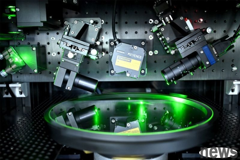
Zhou Chongbin, deputy director of the Department of Industry and Technology of the Ministry of Economic Affairs, said that generative AI and high-speed computing have boosted the data center traffic by more than 70 times from 2010 to 2024, bringing demand for high-speed transmission and high-performance chips. The Technology Corporation has invested nearly 40 billion yuan in the past five years, focusing on AI, high-performance computing (HPC), silicon photons, advanced packaging and compound semiconductors, promoting the soft and hard integration of wafers and the independent manufacturing of advanced manufacturing, and creating a more powerful, technologically advanced semiconductor supply chain in Taiwan that is leading, independent and controllable. Among them, the Industrial Research Institute has successfully developed the first 1.6 Tbps silicon photonic engine module in China. The performance has reached the international level. It has also connected with Sun and Moonlight and other industry players to create a "Silicon Optical Semiconductor Open Platform", providing one-stop service for design, manufacturing, integration and sealing, and accelerating the upgrade of data centers.
Zhou Chongbin also said that the world's first "3D customized chip universal module" will be launched, allowing chips to be quickly combined like wood without zero design, shortening development time and reducing costs. It has served more than 133 businesses and promoted investment of more than 2.1 billion yuan. These achievements not only inject new energy into AIoT, but also strengthen the autonomy and competition of Taiwan's semiconductor supply chain, ensuring that Taiwan continues to play a key role in the global high-speed computing and smart application stage.
Zhang Shijie, deputy director of the Institute of Electrical Research and Optical Systems, said that the Institute of Technology is committed to forward-looking semiconductor and AI technology research and development, and uses system integration thinking to lead the upgrading of the industry chain, showing Taiwan's key energy in the next generation of high-speed computing and intelligent manufacturing. Faced with the rapid rise in global data transmission demand, the traditional optical and electrical architecture has gradually approached the limit. The Industrial and Research Institute took the lead in breaking through the development of the silicon photonic optical engine module, and highly integrates optical components with advanced packaging, not only greatly reduces delays, improves frequency width and efficiency, but also successfully links to create a "silicon optical semiconductor open platform" to help Taiwanese businessmen directly attack the new international blue sea.
On the other hand, the Industrial Research Institute world's first 3D customized chip universal module has shortened the development process that originally took more than half a year to 12 weeks. The module has smaller size but more complete functions. It has successfully transformed Xunchen International and has built trial production lines such as Xingxing Electric and Dingchen Technology to help the industry leapfrog the bottleneck of efficiency and yield, and become an important engine to promote the acceleration of Taiwan's AIoT industry. These achievements not only fill the gap in international technology, but also highlight Taiwan’s leading position in the global semiconductor competition. In the future, the Industrial Research Institute will continue to promote the AI of semiconductors and create a more competitive and competitive industry ecosystem.
According to the Ministry of Economic Affairs, the highlighted technologies of 2025 SEMICON TAIWAN "Technology Research and Development Theme Museum of the Ministry of Economic Affairs" include:
1. Silicon photonic technology international connection acceleration, new milestone for high-speed transmissionThe traditional method requires firstly to send the data of the computing chip to the optical chip through the circuit board and then output, with long transmission paths and limited speed. Through advanced packaging technology of silicon photon combined with advanced packaging technology, the Industrial Research Institute has highly integrated optical components, so that data can be transmitted instantly, greatly reducing delays, improving frequency width and efficiency, laying the foundation for the ultra-high-speed and low-power transmission capabilities required for data center and high-efficiency computing. The Industrial Research Institute successfully developed Taiwan's first 1.6 Tbps silicon photonic light engine module, with performance reaching the Nvidia GTC 2025 international standard. At the same time, the series industry has created a "Silicon Optical Semiconductor Open Platform", combining ultra-high-speed and multi-channel measurement capabilities (224Gbps/Lane) with high-density component design (2.5D/3D), and combined with optical chip heterogeneous packaging, helping operators to quickly develop silicon photonic technology with one-stop service. It has successfully linked design, manufacturing, packaging, quantity testing, equipment and other supply chain partners to strengthen Taiwan's global competitiveness in the next generation of high-speed computing.
2. The world's first universal module for customized 3D chips, small chips promote AIoT to accelerate its launch The development process of System in Package (SiP) lasts for half a year to one year, and the product launch process has been delayed due to repeated verification. The world's first "3D customized chip universal module" was created by the Institute of Technology. Through the pre-made active cutting chip embedded in the connected substrate, it effectively shortens the development time to 12 weeks, improves the efficiency by 70%, and can break through the bottleneck of AIoT products on the market. At the same time, public substrates are formulated to comply with JEDEC international standards to ensure high yield and reduce production complexity. Its elastic design can be versatile with various sensors, and the module is reduced by 30%. It can still integrate multiple IO interfaces, Full-HD image processing, AI high-speed computing and RF transmission to create the world's smallest development board. This technology has not only been successfully applied and transformed into the micro module commissioned by Xunchen International, but also plans to cover 70% of the AIoT market applications. It has also established trial production lines for manufacturers such as Xinxing Electric and Dingchen Technology, and has invested more than 2.1 billion yuan, becoming a Taiwan AIoT industry accelerator..
Because the advanced packaging layer production process is becoming increasingly complex, traditional inspection requires multiple devices, and the relationship between size (2D) and morphology (3D) cannot be grasped at the same time. This module combines 2D microscope and 3D interference into a single optical path equipment, eliminating the removal of multiple stations and re-alignment, reducing detection time by 50%, reducing equipment costs by 40%, and has large-scale (400μm) and nano-level (< 0.5 nm) high analytical analysis capabilities. It has assisted Chengxiang Technology in developing 5G antenna module testing equipment, and has cooperated with Taiwan Siam to develop HAMR hard drive testing equipment to meet the needs of advanced packaging process.
4. Array vision × nano precision: next-generation packaging efficient testing solutionThe advanced packaging of global semiconductor and electronic processes can continue to grow. Due to the demand for improved detection efficiency, the Industrial Research Institute of Technology has created the first miniaturized array lens technology in Taiwan, achieving 2×2 multi-scope automatic micro calibration, which can be used in nano-level testing such as advanced packaging, μLED, passive components and other industrial testing equipment, which is relatively traditional The lens detection system has 4 times the detection vision, maintain high accuracy, and improve detection efficiency by 4 to 10 times. It meets the requirements of nano-level online testing in the process. It has cooperated with domestic equipment manufacturers and system integrators to develop duplex equipment, and has completed the National Institute of Standard Technology (NIST) standard parts, μBump, μLED sample verification.
5. Glass surface particle testing equipment Precise monitoring of transparent Glass qualityThe surface particle detection of the wafer is a key process in the semiconductor process. The current optical detection technology is slow and has insufficient sensitivity, so it cannot meet the needs of transparent wafers and smaller particles. The Institute of Technology has independently developed an oblique incident laser scattering optical module and algorithm, which can detect materials such as silicon, silicon carbide, glass, etc., with a minimum particle size of 0.2 μm. It takes only 4 minutes for an 8-inch crystal circle to complete the test. At present, domestic crystalline factories have been assisted in the introduction of testing applications. Through Shengge Technology and Heya Smart Technology, they are used for glass plates and Semiconductor SiC crystalline online testing, which helps the industry improve yield and reduce costs, and improves the industry's industry vacancy that lacks transparent crystalline detection standards, and helps the development of domestic independent equipment to enhance domestic supply chain.